
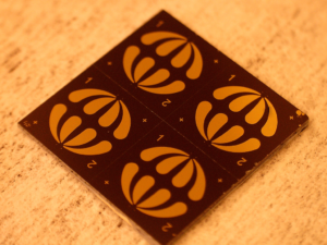
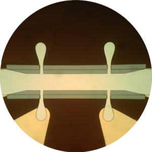
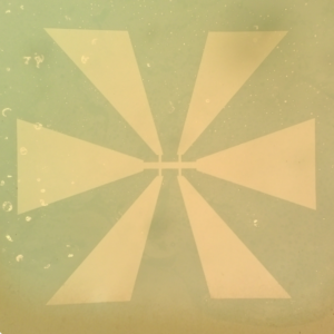
One of the primary uses of the LW405C is defining microcircuit geometries. The image to the right shows an array of four gold contact sets patterned on a scribed silicon wafer. This array was patterned in about 10 minutes on the laser writer and then coated with gold. Once broken apart, each die will be covered with photoresist and patterned with the laser writer again, exposing a microbridge geometry across the ends of the gold pads. The dies will then be sputter coated with granular aluminum oxide and cleaned, leaving metal only where the microbridge pattern was exposed. The edges of the deposited bridge are etched away in another lithographic step followed by broad-beam argon ion milling. The image below shows a completed microbridge. The dark background is the silicon nitride wafer surface. The two gold leads at the bottom of the image will be used to measure a voltage difference as current flows along the sample. The light colored sample is granular aluminum oxide.
This particular film has a superconducting transition temperature of 1.609 K, below which the electrical resistance of the material goes to zero and small magnetic fields are expelled from the bridge. For higher magnetic fields, quantized filaments of magnetic flux force their way into the bridge. These vortices produce a magnet field above the bridge surface that can be measured by a magnetic probe.
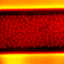
By scanning a small Hall probe just above the bridge, the out-of-plane component of the magnetic field can be measured. The image to the right shows a magnetic micrograph of the middle of the granular aluminum oxide bridge at 1.450 K in a 1.5 G field. The bridge edges are clearly visible because the currents flowing produce relatively large magnetic fields.
–
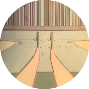
Weston Maughan, a graduate student in physics, used the LW405C to create a superconducting nanowire. The wire will be cooled to ~1 K and scanned with a cryogenic atomic force microscope to investigate the phenomena of phase slips in low-dimension superconductors. The fabrication process requires at least six lithographic exposure steps, each of which much be carefully aligned. The upper portion of the image shows a binary de Bruijn sequence etched into the silicon wafer which is used to determine the position of probe relative to the wire. The gold contacts to the left and right lie along a step etched into the silicon. By depositing superconducting material normal to the substrate surface and then ion milling the material away at an angle, a small filament of material is left in the shadow of the step.
The bridge geometry shown to the left is used extensively to probe material properties such as resistance, carrier mobility and density, and the Hall coefficient. This particular geometry was designed and created by Jinjun Ding of Dr. Mingzhong Wu’s group in the Department of Physics at CSU. The magnetic film was deposited on the sapphire substrate. Photoresist was spun on the film surface and selectively exposed with the LW405C. Once developed, the photoresist only covered the portions of the magnetic film which remain in the image. A broad beam argon ion mill was used to remove the film in the areas not protected by resist. 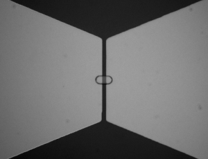 Finally, the resist was removed with acetone leaving the structure shown. This bar will eventually be tested with the physical properties measurement system (PPMS) in the CIF at CSU.
Jinjun Ding also fabricated a Hall bar using the laser lithography facility, shown in the image to the left. This particular Sn/CoFeB bilayer Hall bar has a ~5 μm gap (dark stripe) between the contacts (light grey) and was used to study spin-orbit torque-induced magnetization within this material.
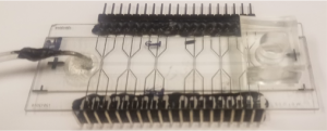
Jasmine Najed, a graduate student working in Dr. Tom Chen’s group, used the laser lithography system to fabricate biosensor electrodes with a liftoff process. The electrodes were patterned in s1813 photoresist and then developed and metalized.